

Facile preparation of a PbS:Ni nanostructure using solid state synthesis route: microstructural, dielectric, and electrical properties
Abstract
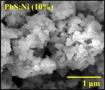
In the present study, a novel PbS:Ni (10 at. %) nanostructure was synthesised via a simple solid state reaction method at 400 °C and constant pressure. X-ray diffraction analysis confirms the formation of a face-centred cubic crystalline structure. Preferential growth is observed along the (311) plane direction. The calculated crystallite size of PbS:Ni (10 at. %) from XRD analysis was found to be equal to 65 nm. Scanning electron microscopy revealed the formation of nanostructured PbS:Ni (10 at. %) materials. Its band gap of ~ 2.14 eV was determined by photoluminescence spectroscopy. Raman spectroscopy was used to confirm the structure of the material. Electrical properties were studied by I-V characteristic at ± 5 V and a temperature range from 100 K to 300 K. The lnV-lnI plot showed a non-linear behaviour of PbS:Ni (10 at. %). Impedance spectroscopy is applied at temperatures from 100 K to 300 K in a frequency range from 20 Hz to 2 MHz to observe the dielectric response of PbS:Ni (10 at. %). As obtained, ε′ ~ 26 and conductivity in the order of 10–4 S · cm–1 were obtained at all temperatures above 104 Hz. The results obtained from photoluminescence spectroscopy, I-V characteristics and impedance spectroscopy confirm that PbS:Ni (10 at. %) can be considered as a suitable material for optoelectronic applications.
Keywords
Full Text:
PDFReferences
Rajashree C, Balu AR, Nagarethinam VS, Properties of cd doped PbS thin films: doping concentration effect, Surf. Eng., 31(4) (2015) 316. https://doi.org/10.1179/1743294415Y.0000000014
Liu X, Zhang M, Studies on PbS and PbSe detectors for IR System, Int. J. Infrared Millim. Waves, 21 (2000) 1697–1701. https://doi.org/10.1023/A:1006676029014
Madelung O. III-V compounds, Semiconductors: Data Handbook. Publisher: Springer; 2004. P. 71–172.
RaviShankar S, Balu AR, Anbarasi M, Nagarethinam VS, Influence of precursor molar concentration on the structural, morphological, optical and electrical properties of PbS thin films deposited by spray pyrolysis technique using perfume atomizer, Optik, 126(20) (2015) 2550–2555. https://doi.org/10.1016/j.ijleo.2015.06.039
Nair PK, Gomezdaza O, Nair MTS, Metal sulphide thin film photography with lead sulphide thin films, Adv. Mater. Opt. Electron., 1(3) (1992) 139–145. https://doi.org/10.1002/amo.860010307
Akhtar S, Saeed N, Hanif MB, Dogar S, et al., PbS and PbO Thin films via e-beam evaporation: Morphology, structure, and electrical properties, Materials, 15(19) (2022) 6884. https://doi.org/10.3390/ma15196884
Li D, Liang C, Liu Y, Qian S, Femtosecond nonlinear optical properities of PbS nanoparticles, J. Lumin., 122–123 (2007) 549–551. https://doi.org/10.1016/j.jlumin.2006.01.214
Gohar O, Khan MZ, Bibi I, Bashir N, et al., Nanomaterials for advanced energy applications: Recent advancements and future trends, Materials & Design, 241 (2024) 112930. https://doi.org/10.1016/j.matdes.2024.112930
Aryamol KS, Kanagaraj K, Nangan S, Haponiuk JT, et al., Recent Advances of carbon Pathways for Sustainable Environment development, Environmental Research, 250 (2024) 118513. https://doi.org/10.1016/j.envres.2024.118513
Naşcu C, Vomir V, Pop I, Ionescu V, et al., The study of lead sulphide films. VI. influence of oxidants on the chemically deposited PbS thin films, Mater. Sci. Eng.: B, 41(2) (1996) 235–240. https://doi.org/10.1016/S0921-5107(96)01611-X
Larramendi EM, Calzadilla O, González-Arias A, Hernández E, et al., Effect of surface structure on photosensitivity in chemically deposited PbS thin films, Thin Solid Films, 389(1–2) (2001) 301–306. https://doi.org/10.1016/S0040-6090(01)00815-X
Pentia E, Pintilie L, Tivarus C, Pintilie I, et al., Influence of Sb3+ ions on photoconductive properties of chemically deposited PbS films, Mater. Sci. Eng.: B, 80(1–3) (2001) 23–26. https://doi.org/10.1016/S0921-5107(00)00578-X
Joshi RK, Kanjilal A, Sehgal HK, Solution grown PbS nanoparticle films, Appl. Surf. Sci., 221(1–4) (2004) 43–47. https://doi.org/10.1016/S0169-4332(03)00955-3
Valenzuela-Jáuregui JJ, Ramı́rez-Bon R, Mendoza-Galván A, Sotelo-Lerma M, Optical properties of PbS thin films chemically deposited at different temperatures, Thin Solid Films, 441(1–2) (2003) 104–110. https://doi.org/10.1016/S0040-6090(03)00908-8
Thangaraju B, Kaliannan P, Spray pyrolytically deposited PbS thin films, Semicond. Sci. Technol., 15 (2000) 849. https://doi.org/10.1088/0268-1242/15/8/311
Sharon M, Ramaiah KS, Kumar M, Neumann-Spallart M et al., Electrodeposition of lead sulphide in acidic medium, J. Electroanal. Chem., 436(1–2) (1997) 49–52. https://doi.org/10.1016/S0022-0728(97)00124-1
Slonopas A, Alijabbari N, Saltonstall C, Globus T, et al., Chemically deposited nanocrystalline lead sulfide thin films with tunable properties for use in photovoltaics, Electrochimica Acta, 151 (2015) 140–149. https://doi.org/10.1016/j.electacta.2014.11.021
Ni Y, Wang F, Liu H, Yin G, et al., A novel aqueous-phase route to prepare flower-shaped PbS micron crystals, J. Cryst. Growth, 262(1–4) (2004) 399–402. https://doi.org/10.1016/j.jcrysgro.2003.10.053
Zhao Y, Liao XH, Hong JM, Zhu JJ, Synthesis of lead sulfide nanocrystals via microwave and sonochemical methods, Mater. Chem. Phys., 87(1) (2004) 149–153. https://doi.org/10.1016/j.matchemphys.2004.05.026
Springholz G, Bauer G, Investigation of Pb1−xEuxTe molecular beam epitaxy by reflection high-energy electron diffraction intensity oscillations, Appl. Phys. Lett., 60(13) (1992) 1600. https://doi.org/10.1063/1.107238
Wang H, Zhang JR, Zhu JJ, Sonochemical preparation of lead sulfide nanocrystals in an oil-in-water microemulsion, J. Cryst. Growth, 246(1–2) (2002) 161–168. https://doi.org/10.1016/S0022-0248(02)01808-0
Zhang W, Yang Q, Xu L, Yu W, et al., Growth of PbS crystals from nanocubes to eight-horn-shaped dendrites through a complex synthetic route, Mater. Lett., 59(27) (2005) 3383–3388. https://doi.org/10.1016/j.matlet.2004.09.065
Nazir A, Toma A, Shah NA, Panaro S, et al., Effect of ag doping on opto-electrical properties of CdS thin films for solar cell applications, J. Alloys Compd., 609 (2014) 40–45. https://doi.org/10.1016/j.jallcom.2014.04.144
Kaci S, Keffous A, Hakoum S, Mansri A, Hydrogen sensitivity of the sensors based on nanostructured lead sulfide thin films deposited on a-SiC:H and p-Si(100) substrates, Vacuum, 116 (2015) 27–30. https://doi.org/10.1016/j.vacuum.2015.02.024
Sultan A, Ahmad M, Imran Z, Batool SS, et al., Tailoring structural, dielectric and optical effects of PbS nanosheets with ni doping, Phys. B: Condens. Matter, 602 (2021) 412571. https://doi.org/10.1016/j.physb.2020.412571
Hussain A, Begum A, Rahman A, Electrical and optical properties of nanocrystalline lead sulphide thin films prepared by chemical bath deposition, Indian J. Phys., 86 (2012) 697–701. https://doi.org/10.1007/s12648-012-0130-2
Rajashree C, Balu AR, Tuning the physical properties of PbS thin films towards optoelectronic applications through Ni doping, Optik, 127(20) (2016) 8892–8898. https://doi.org/10.1016/j.ijleo.2016.06.106
Garcia OP, Albuquerque MCC, Aquino KAS, Araujo PLB, et al., Use of lead (II) sulfide Nanoparticles as stabilizer for PMMA exposed to gamma Irradiation, Mater. Res., 18(2) (2015) 365. https://doi.org/10.1590/1516-1439.330214
Navaneethan M, Nisha KD, Ponnusamy S, Muthamizhchelvan C, Optical and surface morphological properties of triethylamine passivated lead sulphide nanoparticles, Mater. Chem. Phys., 117(2–3) (2009) 443–447. https://doi.org/10.1016/j.matchemphys.2009.06.026
Parveen A, Agrawal S, Azam A, Band gap tuning and fluorescence properties of lead sulfide Pb0.9A0.1S (A: Fe, Co, and Ni) nanoparticles by transition metal doping, Opt. Mater., 76 (2018) 21–27. https://doi.org/10.1016/j.optmat.2017.12.015
Langford JI, Wilson AJC, Scherrer after sixty years: A survey and some new results in the determination of crystallite size, J. Appl. Crystallogr., 11 (1978) 102–113. https://doi.org/10.1107/S0021889878012844
Rajashree C, Balu AR, Nagarethinam VS, Properties of cd doped PbS thin films: doping concentration effect, Surf. Eng., 31(4) (2015) 316. https://doi.org/10.1179/1743294415Y.0000000014
Priyanka U, Akshay Gowda KM, Elisha MG, Surya Teja B, et al., Biologically synthesized PbS nanoparticles for the detection of arsenic in water, Int. Biodeterior. & Biodegradation, 119 (2017) 78–86. https://doi.org/10.1016/j.ibiod.2016.10.009
Smith GD, Firth S, Clark RJH, Cardona M, First- and second-order Raman spectra of galena (PbS), J. Appl. Phys., 92(8) (2002) 4375–4380. https://doi.org/10.1063/1.1505670
Shapter JG, Brooker MH, Skinner WM, Observation of the oxidation of galena using Raman spectroscopy, Int. J. Miner. Process., 60(3–4) (2000) 199–211. https://doi.org/10.1016/S0301-7516(00)00017-X
Chiu FC, A review on conduction Mechanisms in dielectric Films, Adv. Mater. Sci. Eng., 2014 (2014) 1. https://doi.org/10.1155/2014/578168
Ahmad M, Rafiq MA, Hasan MM, Transport characteristics and colossal dielectric response of cadmium sulfide nanoparticles, J. Appl. Phys., 114 (2013) 133702. https://doi.org/10.1063/1.4823810
Afsar MF, Jamil A, Rafiq MA, Ferroelectric, dielectric and electrical behavior of two-dimensional lead sulphide nanosheets, Adv. Nat. Sci.: Nanosci. Nanotechnol., 8 (2017) 045010. https://doi.org/10.1088/2043-6254/aa8b3d
Rasool K, Rafiq MA, Li CB, Krali E, et al., Enhanced electrical and dielectric properties of polymer covered silicon nanowire arrays, Appl. Phys. Lett., 101 (2012) 023114. https://doi.org/10.1063/1.4735278
Batoo KM, Kumar S, Lee CG, Alimuddin, Finite size effect and influence of temperature on electrical properties of nanocrystalline Ni–Cd ferrites, Curr. Appl. Phys., 9(5) (2009) 1072–1078. https://doi.org/10.1016/j.cap.2008.12.002
Sathishkumar G, Venkataraju C, Sivakumar K, Synthesis, structural and dielectric Studies of nickel Substituted Cobalt-Zinc Ferrite, Mater. Sci. Appl., 1(1) (2010) 19–24. https://doi.org/10.4236/msa.2010.11004
Koops CG, On the dispersion of resistivity and dielectric Constant of some Semiconductors at Audiofrequencies, Phys. Rev., 83 (2002) 121. https://doi.org/10.1103/PhysRev.83.121
Zhou SM, Dielectric properties of phase-size-control CdS nanoparticles and conventional powders, Phys. status solidi (a), 200(2) (2003) 423–428. https://doi.org/10.1002/pssa.200306687
Batool SS, Imran Z, Rafiq MA, Hasan MM, et al., Investigation of dielectric relaxation behavior of electrospun titanium dioxide nanofibers using temperature dependent impedance spectroscopy, Ceram. Int., 39(2) (2013) 1775–1783. https://doi.org/10.1016/j.ceramint.2012.08.024
Costa MM, Pires GFM, Terezo AJ, Graça MPF, et al., Impedance and modulus studies of magnetic ceramic oxide Ba2Co2Fe12O22 (Co2Y) doped with Bi2O3, J. Appl. Phys., 110(3) (2011) 034107. https://doi.org/10.1063/1.3615935
Ahmad M, Rafiq MA, Imran Z, Rasool K, et al., Charge conduction and relaxation in MoS2 nanoflakes synthesized by simple solid state reaction, J. Appl. Phys., 114(4) (2013) 043710. https://doi.org/10.1063/1.4816570
Liu M, Zhan Q, Li W, Li R, et al., Effect of Zn doping concentration on optical band gap of PbS thin films, J. Alloys Compd., 792 (2019) 1000–1007. https://doi.org/10.1016/j.jallcom.2019.04.117
Vankhade D, Kothari A, Chaudhuri TK, Direct-coated Photoconducting nanocrystalline PbS thin Films with tunable Band Gap, J. Electron. Mater., 45 (2016) 2789–2795. https://doi.org/10.1007/s11664-016-4364-1
Dey P, Paul J, Bylsma J, Karaiskaj D, et al., Origin of the temperature dependence of the band gap of PbS and PbSe quantum dots, Solid State Commun., 165 (2013) 49–54. https://doi.org/10.1016/j.ssc.2013.04.022
Nanda KK, Kruis FE, Fissan H, Acet M, Band-gap tuning of PbS nanoparticles by in-flight sintering of size classified aerosols, J. Appl. Phys., 91(4) (2002) 2315–2321. https://doi.org/10.1063/1.1431429
Jana S, Thapa R, Maity R, Chattopadhyay KK, Optical and dielectric properties of PVA capped nanocrystalline PbS thin films synthesized by chemical bath deposition, Phys. E: Low-Dimens. Syst. Nanostructures, 40(10) (2008) 3121–3126. https://doi.org/10.1016/j.physe.2008.04.015
Shkir M, Chandekar KV, Hossain MM, Palanivel B, et al., Enhanced dielectric and electrical properties of PbS nanostructures facilely synthesized by low-cost chemical route: an effect of Ce doping concentrations, Mater. Chem. Phys., 278 (2022) 125626. https://doi.org/10.1016/j.matchemphys.2021.125626
Chandekar KV, Alshahrani T, Ben Gouider Trabelsi A, Alkallas FH, et al., Novel rare earth yttrium doping effect on physical properties of PbS nanostructures: facile synthesis and characterization, J. Mater. Sci., 56 (2021) 4763–4781. https://doi.org/10.1007/s10853-020-05539-w
Trabelsi ABG, Alkallas FH, Chandekar KV, Kumar A, et al., Facile low temperature development of Ag-doped PbS nanoparticles for optoelectronic applications, Materials Chemistry and Physics, 297, (2023) 127299. https://doi.org/10.1016/j.matchemphys.2023.127299
Mariappan SM, Hong SJ, Han B, Shkir M, et al., Slow excitonic carrier cooling in Sr-doped PbS nanocrystals for hot carrier devices: an integrated experimental and first-principles approach, Journal of Materials Chemistry C, 10 (2022) 6634–6645. https://doi.org/10.1039/D1TC05921A
Shkir M, Chandekar KV, Khan A, El-Toni AM, et al., A facile synthesis of Bi@PbS nanosheets and their key physical properties analysis for optoelectronic technology, Materials Science in Semiconductor Processing, 107 (2020) 104807. https://doi.org/10.1016/j.mssp.2019.104807
Shkir M, Khan M T, Ashraf I M, AlFaify S, et al., Rapid microwave-assisted synthesis of Ag-doped PbS nanoparticles for optoelectronic applications, Ceramics International, 45(17) (2019) 21975–21985. https://doi.org/10.1016/j.ceramint.2019.07.212
Shkir M, AlFaify S, A facile low-temperature synthesis of nanosheets assembled PbS microflowers and their structural, morphological, optical, photoluminescence, dielectric and electrical studies, Materials Research Express, 6 (2019) 105013. https://doi.org/10.1088/2053-1591/ab3535
Shkir M, Yahia IS, AlFaify S, A facilely one pot low temperature synthesis of novel Pt doped PbS nanopowders and their characterizations for optoelectronic applications, Journal of Molecular Structure, 1192 (2019) 68–75. https://doi.org/10.1016/j.molstruc.2019.04.099
Shkir M, Ashraf IM, AlFaify S, Surface area, optical and electrical studies on PbS nanosheets for visible light photo-detector application, Physica Scripta, 94 (2019) 025801. https://doi.org/10.1088/1402-4896/aaf55a
Hanif MB, Rauf S, Sultan A, Tayyab Z, et al., Boosting the electrochemical performance of oxygen electrodes via the formation of LSCF-BaCe0.9–xMoxY0.1O3–δ triple conducting composite for solid oxide fuel cells: Part II., Energy, 289 (2024) 129985. https://doi.org/10.1016/j.energy.2023.129985
Khan K, Qayyum S, Hanif MB, Rauf S, et al., Design of efficient and durable symmetrical protonic ceramic fuel cells at intermediate temperatures via B-site doping of Ni in BaCe0.56Zr0.2Ni0.04Y0.2O3–δ, Ceramics International, 49(11) (2023) 16826–16835. https://doi.org/10.1016/j.ceramint.2023.02.043
DOI: https://doi.org/10.15826/elmattech.2024.3.033
Copyright (c) 2024 Amir Sultan, Mushtaq Ahmad, Muhammad Zubair Khan, Junaid ur Rehman, Zahid Imran, Muhammad Bilal Hanif, Martin Motola

This work is licensed under a Creative Commons Attribution 4.0 International License.
![]()
![]()
![]()
![]()
![]()